
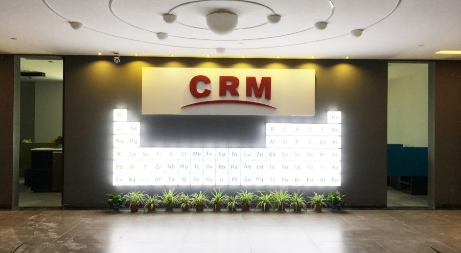

- H氢
- He氦
- Li锂
- Be铍
- B硼
- C碳
- N氮
- O氧
- F氟
- Ne氖
- Na钠
- Mg镁
- Al铝
- Si硅
- P磷
- S硫
- Cl氯
- Ar氩
- K钾
- Ca钙
- Sc钪
- Ti钛
- V钒
- Cr铬
- Mn锰
- Fe铁
- Co钴
- Ni镍
- Cu铜
- Zn锌
- Ga镓
- Ge锗
- As砷
- Se硒
- Br溴
- Kr氪
- Rb铷
- Sr锶
- Y钇
- Zr锆
- Nb铌
- Mo钼
- Tc碍
- Ru钌
- Rh铑
- Pd钯
- Ag银
- Cd镉
- In铟
- Sn锡
- Sb锑
- Te碲
- I碘
- Xe氙
- Cs铯
- Ba钡
- LaLu镧系
- Hf铪
- Ta钽
- W钨
- Re铼
- Os锇
- Ir铱
- Pt铂
- Au金
- Hg汞
- Tl铊
- Pb铅
- Bi铋
- Po钋
- At砹
- Rn氡
- La镧
- Ce铈
- Pr镨
- Nd钕
- Pm钷
- Sm钐
- Eu铕
- Gd钆
- Tb铽
- Dy镝
- Ho钬
- Er铒
- Tm铥
- Yb镱
- Lu镥
点击可查看包含对应元素的相关产品信息
科泰新材料可提供“元索周期表”近乎全元素(除放射性元素外)的任意组合材料定制,
部分产品未及时更新,特殊定制需求请咨询客服。
- Al铝
- Ar氩
- As砷
- Ag银
- Au金
- At砹
- Be铍
- B硼
- Br溴
- Ba钡
- Bi铋
- C碳
- Cl氯
- Ca钙
- Cr铬
- Co钴
- Cu铜
- Cd镉
- Cs铯
- Ce铈
- Dy镝
- Eu铕
- Er铒
- F氟
- Fe铁
- Ga镓
- Ge锗
- Gd钆
- H氢
- He氦
- Hf铪
- Hg汞
- Ho钬
- In铟
- I碘
- Ir铱
- K钾
- Kr氪
- Li锂
- LaLu镧系
- La镧
- Lu镥
- Mg镁
- Mn锰
- Mo钼
- N氮
- Ne氖
- Na钠
- Ni镍
- Nb铌
- Nd钕
- O氧
- Os锇
- P磷
- Pd钯
- Pt铂
- Pb铅
- Po钋
- Pr镨
- Pm钷
- Rb铷
- Re铼
- Rn氡
- Ru钌
- Rh铑
- Si硅
- S硫
- Sc钪
- Se硒
- Sr锶
- Sn锡
- Sb锑
- Te碲
- Sm钐
- Ti钛
- Tc碍
- Ta钽
- Tl铊
- Tb铽
- Tm铥
- V钒
- W钨
- Xe氙
- Yb镱
- Y钇
- Zn锌
- Zr锆
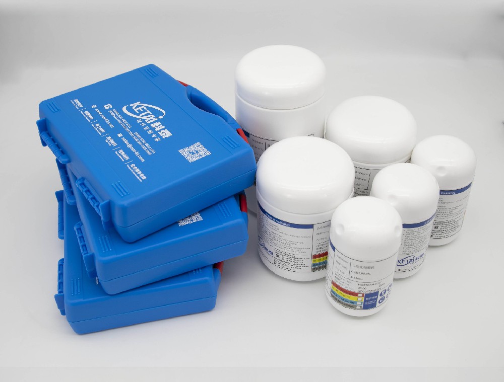
产品中心
PRODUCTS

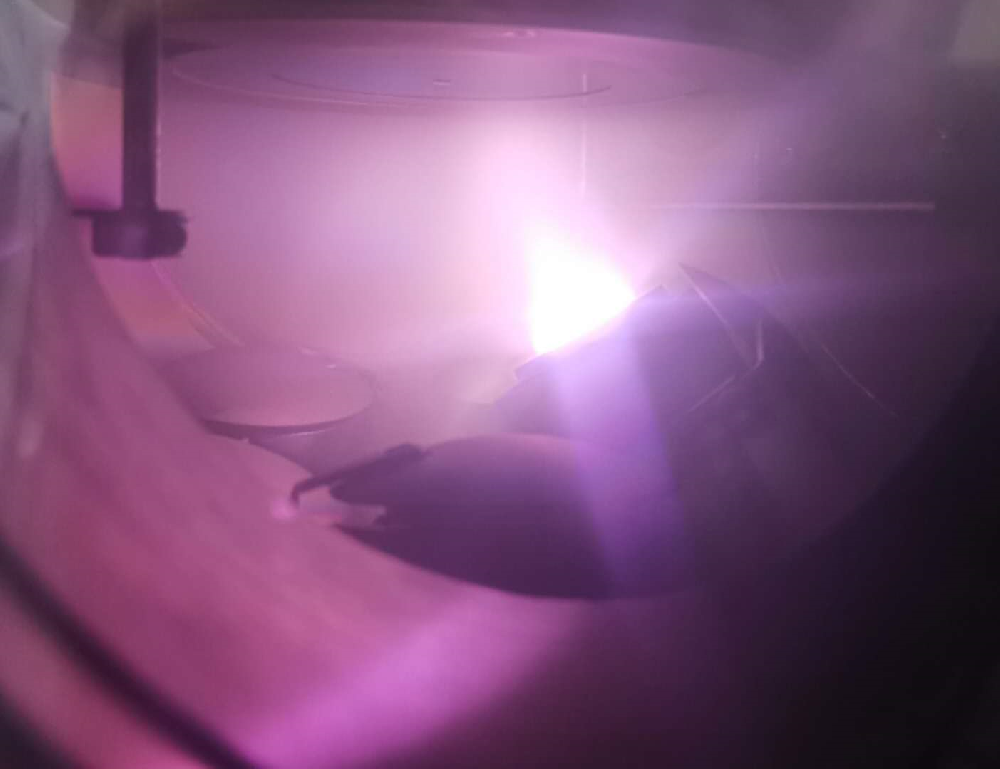
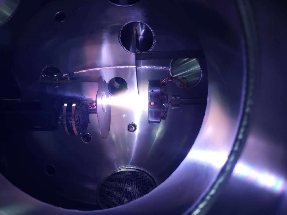
二硅化钇靶材(YSi2)
")
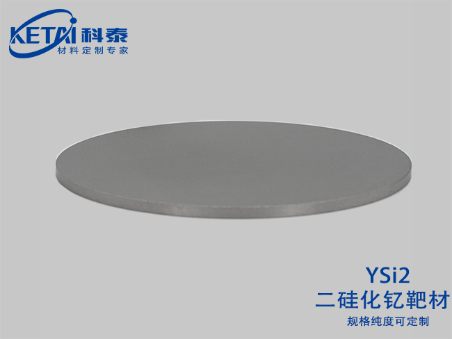
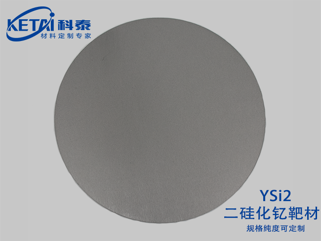
| 二硅化钇靶材(YSi2)基本信息 | |
| 分子式 | YSi2 |
| 纯度 | 99.5% |
| CAS号 | |
| 摩尔质量 | |
| 密度 | |
| 熔点 | |
| 沸点 | |
| 溶解性(水) | |
二硅化钇靶材(YSi2)产品概况
二硅化钇靶材以高纯钇锭(99.995%)与半导体级硅粉为原料,经真空电弧熔炼→氢化歧化(HDDR)→放电等离子烧结(SPS)制备,核心价值在于超高温稳定性(熔点>2200℃)、低活化特性(核废料半衰期<10年)及独特电导率(>1000 S/cm),专用于第四代核反应堆中子倍增层、航天发动机热障涂层(TBCs)、量子芯片铜互连阻挡层及极端环境传感器电极。通过晶界氧捕捉(Y-Si-O玻璃相)、层状MAX相复合(YSi₂/Y₂AlC)及织构定向调控,突破硅挥发损耗与辐照肿胀瓶颈。
| 二硅化钇靶材(YSi2)产品应用 |
◉ 百万比特超导量子芯片
YBCO/YSi₂异质结量子比特
超导相干时间 75μs@8T(传统铝基芯片5.3倍)
量子门操作精度 99.999%(突破容错计算阈值)
极低温电磁屏蔽
YSi₂涡流损耗 <10⁻¹⁸ W/μm²(抑制磁通噪声)
◉ 聚变堆第一壁装甲革命
抗中子嬗变防护层
嬗变毒化物累积 <1ppm(ITER全周期)
热负荷能力 45MW/m²(钨材料的1.8倍)
氚增殖包层
Li-YSi₂复合层:氚增殖率 TBR=1.52(突破能量自持阈值)
◉ 1nm芯片光刻光学系统
深紫外折反混合镜头
193nm波前畸变 <λ/100(支撑ASML Hyper-NA)
热变形系数 0.03nm/K(晶圆套刻精度↑90%)
光子晶体缺陷修复
YSi₂@SiO₂光子筛:套刻误差 <0.15nm
")
")
")
")
产品需求
PRODUCT DEMAND

-

微信扫一扫实时报价
-

微信公众号
-

关注微信视频号
-

抖音扫码,加我好友